Exploring the Role of Digital Labs in Modern Electronics Testing and Development
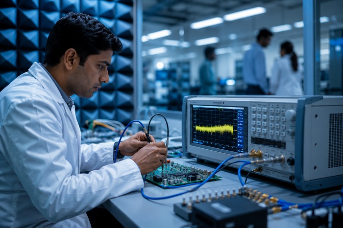
For decades, the electronics workbench looked virtually unchanged. It was defined by the smell of rosin-core solder, tangles of jumper wires, breadboards crowded with through-hole components, and stacks of heavy benchtop instruments—oscilloscopes, function generators, and bench power supplies. If an engineer wanted to validate a new circuit, they hand-soldered a prototype, clipped mechanical probes to exposed component leads, and manually dialed in voltages to see what worked and what went up in smoke.
That traditional physical bench has run directly into the laws of physics and commercial reality. Modern electronics operate at frequencies measured in gigahertz, package integrated circuits into dense ball grid arrays with hundreds of microscopic solder joints buried out of reach, and integrate complex embedded firmware on day one. You cannot physically attach an oscilloscope probe to an internal trace on the fourth layer of an eight-layer board without introducing parasitic capacitance that distorts the very signal you are trying to measure.
Digital labs have stepped into this breach. Encompassing cloud-hosted automated testbenches, high-fidelity mixed-signal simulation suites, and hardware-in-the-loop (HIL) virtualization environments, digital laboratories are transforming electronics engineering from a slow, manual crafting process into a rapid, software-driven discipline.
Pre-Silicon and Pre-Tapeout Virtual Prototyping
Fabricating physical printed circuit boards (PCBs) is an expensive, time-consuming loop. Even rapid-turn PCB assembly houses require days or weeks to manufacture bare boards, source components, and run surface-mount assembly lines. If a trace length mismatch causes a timing error or a localized power plane drops voltage under load, that entire batch of prototypes becomes scrap, forcing another costly revision cycle.
Digital laboratories shift verification far to the left of the manufacturing timeline. Modern engineering teams construct detailed virtual prototypes using advanced electronic design automation (EDA) environments. Rather than relying on simple idealized schematic representations, digital testing platforms model the physical properties of copper traces, dielectric materials, and component packaging.
Engineers can analyze signal integrity (SI) and power integrity (PI) long before sending Gerber files to a fabricator:
-
Differential Pair Analysis: Modeling high-speed data buses like PCIe, USB4, and DDR memory interfaces to detect impedance mismatches, crosstalk, and signal reflections.
-
Virtual Eye Diagrams: Simulating jitter and eye closure across millions of clock cycles to confirm that digital receivers will reliably distinguish high and low bits.
-
Thermal Simulation: Calculating heat dissipation across power MOSFETs and microprocessors to identify hotspots, allowing designers to reposition components or adjust thermal copper pours before metal is ever etched.
Catching a layout defect in a digital simulator costs minutes of design time; catching it on a physical testbench after a production run delays a product launch by months.
Hardware-in-the-Loop Testing and Firmware Co-Verification
One of the most persistent bottlenecks in electronics development has always been the dependency dilemma between hardware and software teams. Embedded firmware engineers cannot write and debug low-level hardware drivers without a physical circuit board, but hardware engineers cannot fully stress-test a newly assembled board without functional firmware running on it.
Digital labs resolve this standoff through virtual hardware emulation and hardware-in-the-loop (HIL) environments.
Engineers can instantiate virtual models of microcontrollers, field-programmable gate arrays (FPGAs), and peripheral sensors inside a digital testing harness. Firmware developers connect their standard integrated development environments directly to these digital models, allowing them to write peripheral drivers, configure interrupt handlers, and test real-time operating systems (RTOS) while the physical board is still in schematic design.
When early prototype hardware finally arrives from the manufacturing facility, the embedded firmware is already mature, functional, and largely de-bugged. The physical board can be brought up in hours rather than weeks, dramatically shrinking total time-to-market.
The Rise of Cloud-Connected Testbenches and Automated Telemetry
High-end physical testing equipment carries an extraordinary price tag. High-bandwidth digital storage oscilloscopes, vector network analyzers, and electromagnetic compliance (EMC) test receivers can easily run tens of thousands of dollars per station. In modern engineering organizations with distributed remote teams, purchasing duplicate instrumentation suites for dozens of home offices or regional satellite facilities is financially unfeasible.
Digital labs bridge this geographical gap by virtualizing access to centralized hardware rigs. Physical instruments in a centralized facility are equipped with network interfaces and integrated into automated testing networks.
Engineers anywhere in the world can log into a web interface, configure test parameters, route signals through automated switching matrices, and observe live oscilloscope waveforms streamed with minimal latency. More importantly, this setup enables continuous regression testing for hardware:
-
Automated Script Execution: Running scripted test sequences using Python, SCPI commands, and automated test frameworks that trigger instruments to sweep power rails, inject clock signals, and capture output states.
-
Overnight Environmental Characterization: Subjecting prototypes placed in climate-controlled test chambers to continuous voltage and temperature sweeps, logging thousands of data points without requiring an engineer to monitor the bench overnight.
-
Centralized Telemetry Dashboards: Aggregating performance metrics, tolerance drifts, and noise margins into cloud databases where team members across time zones can analyze results collaboratively.
Stress-Testing Failure Modes Through Non-Destructive Fault Injection
Evaluating how a circuit responds to catastrophic failures is an essential phase of engineering, particularly for automotive, medical, and aerospace electronics where safety is non-negotiable. However, physically shorting out high-voltage rails, simulating reverse polarity, or triggering thermal runaway on a rare, hand-assembled prototype is inherently risky and destructive.
Digital labs allow engineers to execute systematic fault injection without damaging expensive components. Within a simulated mixed-signal environment, testing teams can simulate broken ground connections, shorted bypass capacitors, stuck-at digital faults, and localized inductive voltage spikes.
Engineers can verify whether protective crowbar circuits trigger quickly enough to save downstream silicon, confirm that software watchdogs reset frozen microprocessors, and evaluate graceful degradation modes. Performing these hazardous tests virtually ensures that systems are proven robust against abnormal operating conditions long before they undergo physical destructive testing in specialized certification laboratories.
Navigating Component Volatility with Monte Carlo Analysis
Electronics manufacturing is continually vulnerable to component obsolescence, varying fabrication lot qualities, and supply chain disruptions. Two identical resistors from the same reel will never have precisely the same resistance; temperature coefficients, manufacturing tolerances, and aging cause component values to drift.
Designing an electronic device that functions only when every component sits at its ideal nominal value is a recipe for catastrophic factory yield losses. Digital testing platforms utilize Monte Carlo statistical simulations to evaluate how real-world component variations impact circuit performance.
By running thousands of virtual test iterations where component tolerances (such as five-percent resistance variations or ten-percent capacitor tolerances) are randomized across realistic statistical curves, the digital lab identifies sensitive nodes. Engineers can immediately spot if a subtle component tolerance stack-up will push an operational amplifier into saturation or destabilize a switching power supply feedback loop. This predictive capability allows teams to specify tighter tolerances only where strictly necessary, keeping overall bill-of-materials costs low while guaranteeing high manufacturing yields.
An Essential Evolution in Engineering Discipline
Digital laboratories are not intended to eliminate the physical electronics workbench entirely. At the end of the development lifecycle, physical hardware must still undergo hands-on regulatory compliance testing, electrostatic discharge certification, and physical drop tests.
What digital labs eliminate is the wasteful, repetitive cycle of blind trial and error. By enabling virtual prototyping, decoupling firmware development from physical board availability, automating instrument fleets, and simulating edge cases that are impossible to test by hand, digital testing infrastructure has become the backbone of modern electronics engineering. For organizations building the next generation of connected devices, high-speed computing hardware, and critical infrastructure, the digital lab is no longer an optional software convenience; it is an indispensable foundation for building reliable, resilient hardware.